- 您现在的位置:买卖IC网 > Sheet目录3882 > PIC18F1320T-E/ML (Microchip Technology)IC MCU FLASH 4KX16 EEPROM 28QFN
2007 Microchip Technology Inc.
DS39605F-page 9
PIC18F1220/1320
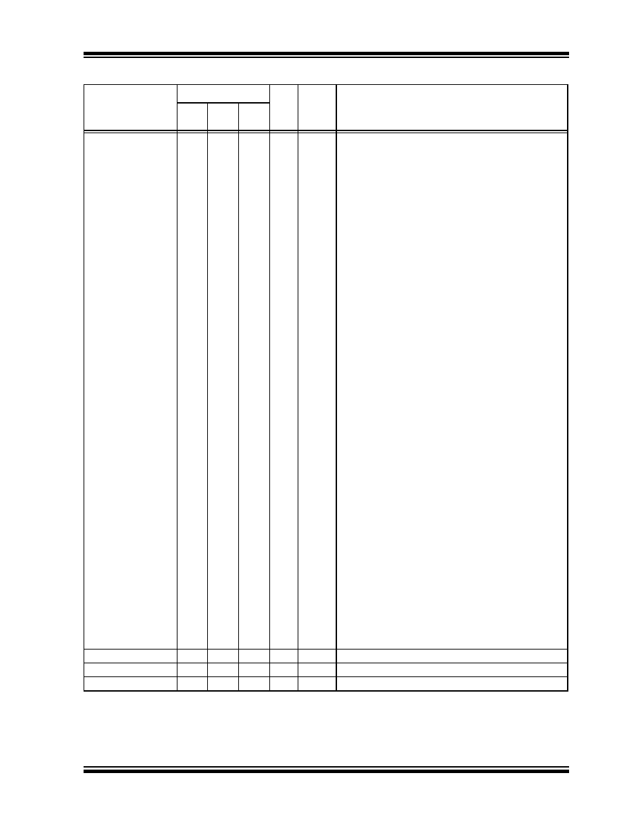
PORTB is a bidirectional I/O port. PORTB can be software
programmed for internal weak pull-ups on all inputs.
RB0/AN4/INT0
RB0
AN4
INT0
89
9
I/O
I
TTL
Analog
ST
Digital I/O.
Analog input 4.
External interrupt 0.
RB1/AN5/TX/CK/INT1
RB1
AN5
TX
CK
INT1
910
10
I/O
I
O
I/O
I
TTL
Analog
—
ST
Digital I/O.
Analog input 5.
EUSART asynchronous transmit.
EUSART synchronous clock (see related RX/DT).
External interrupt 1.
RB2/P1B/INT2
RB2
P1B
INT2
17
19
23
I/O
O
I
TTL
—
ST
Digital I/O.
Enhanced CCP1/PWM output.
External interrupt 2.
RB3/CCP1/P1A
RB3
CCP1
P1A
18
20
24
I/O
O
TTL
ST
—
Digital I/O.
Capture 1 input/Compare 1 output/PWM 1 output.
Enhanced CCP1/PWM output.
RB4/AN6/RX/DT/KBI0
RB4
AN6
RX
DT
KBI0
10
11
12
I/O
I
I/O
I
TTL
Analog
ST
TTL
Digital I/O.
Analog input 6.
EUSART asynchronous receive.
EUSART synchronous data (see related TX/CK).
Interrupt-on-change pin.
RB5/PGM/KBI1
RB5
PGM
KBI1
11
12
13
I/O
I
TTL
ST
TTL
Digital I/O.
Low-Voltage ICSP Programming enable pin.
Interrupt-on-change pin.
RB6/PGC/T1OSO/
T13CKI/P1C/KBI2
RB6
PGC
T1OSO
T13CKI
P1C
KBI2
12
13
15
I/O
O
I
O
I
TTL
ST
—
ST
—
TTL
Digital I/O.
In-Circuit Debugger and ICSP programming clock pin.
Timer1 oscillator output.
Timer1/Timer3 external clock output.
Enhanced CCP1/PWM output.
Interrupt-on-change pin.
RB7/PGD/T1OSI/
P1D/KBI3
RB7
PGD
T1OSI
P1D
KBI3
13
14
16
I/O
I
O
I
TTL
ST
CMOS
—
TTL
Digital I/O.
In-Circuit Debugger and ICSP programming data pin.
Timer1 oscillator input.
Enhanced CCP1/PWM output.
Interrupt-on-change pin.
VSS
5
5, 6
3, 5
P
—
Ground reference for logic and I/O pins.
VDD
14
15, 16 17, 19
P
—
Positive supply for logic and I/O pins.
NC
—
18
—
No connect.
TABLE 1-2:
PIC18F1220/1320 PINOUT I/O DESCRIPTIONS (CONTINUED)
Pin Name
Pin Number
Pin
Type
Buffer
Type
Description
PDIP/
SOIC
SSOP
QFN
Legend:
TTL =
TTL compatible input
CMOS = CMOS compatible input or output
ST
=
Schmitt Trigger input with CMOS levels
I
= Input
O=
Output
P
= Power
OD
=
Open-drain (no P diode to VDD)
发布紧急采购,3分钟左右您将得到回复。
相关PDF资料
PIC16LF87T-I/ML
IC MCU FLASH 4KX14 EEPROM 28QFN
PIC18F25J10-I/SS
IC PIC MCU FLASH 16KX16 28SSOP
PIC16F88T-E/SS
IC MCU FLASH 4KX14 EEPROM 20SSOP
PIC16C621A-04/SO
IC MCU OTP 1KX14 COMP 18SOIC
PIC16F88T-E/ML
IC MCU FLASH 4KX14 EEPROM 28QFN
PIC16F88T-E/SO
IC MCU FLASH 4KX14 EEPROM 18SOIC
PIC16F882-I/SO
IC PIC MCU FLASH 2KX14 28SOIC
PIC16F87T-E/SS
IC MCU FLASH 4KX14 EEPROM 20SSOP
相关代理商/技术参数
PIC18F1320T-E/SO
制造商:Microchip Technology Inc 功能描述:PIC18 Series 256 B RAM 8 kB Flash 8-Bit Enhanced Microcontroller - SOIC-18
PIC18F1320T-I/ML
功能描述:8位微控制器 -MCU 8KB 256 RAM 16 I/O RoHS:否 制造商:Silicon Labs 核心:8051 处理器系列:C8051F39x 数据总线宽度:8 bit 最大时钟频率:50 MHz 程序存储器大小:16 KB 数据 RAM 大小:1 KB 片上 ADC:Yes 工作电源电压:1.8 V to 3.6 V 工作温度范围:- 40 C to + 105 C 封装 / 箱体:QFN-20 安装风格:SMD/SMT
PIC18F1320T-I/SO
功能描述:8位微控制器 -MCU 8KB 256 RAM 16 I/O RoHS:否 制造商:Silicon Labs 核心:8051 处理器系列:C8051F39x 数据总线宽度:8 bit 最大时钟频率:50 MHz 程序存储器大小:16 KB 数据 RAM 大小:1 KB 片上 ADC:Yes 工作电源电压:1.8 V to 3.6 V 工作温度范围:- 40 C to + 105 C 封装 / 箱体:QFN-20 安装风格:SMD/SMT
PIC18F1320T-I/SOG
功能描述:8位微控制器 -MCU 8KB 256 RAM 16 I/O Lead Free Package RoHS:否 制造商:Silicon Labs 核心:8051 处理器系列:C8051F39x 数据总线宽度:8 bit 最大时钟频率:50 MHz 程序存储器大小:16 KB 数据 RAM 大小:1 KB 片上 ADC:Yes 工作电源电压:1.8 V to 3.6 V 工作温度范围:- 40 C to + 105 C 封装 / 箱体:QFN-20 安装风格:SMD/SMT
PIC18F1320T-I/SS
功能描述:8位微控制器 -MCU 8KB 256 RAM 16 I/O RoHS:否 制造商:Silicon Labs 核心:8051 处理器系列:C8051F39x 数据总线宽度:8 bit 最大时钟频率:50 MHz 程序存储器大小:16 KB 数据 RAM 大小:1 KB 片上 ADC:Yes 工作电源电压:1.8 V to 3.6 V 工作温度范围:- 40 C to + 105 C 封装 / 箱体:QFN-20 安装风格:SMD/SMT
PIC18F1330-E/ML
功能描述:8位微控制器 -MCU 8KB Flash 256 RAM RoHS:否 制造商:Silicon Labs 核心:8051 处理器系列:C8051F39x 数据总线宽度:8 bit 最大时钟频率:50 MHz 程序存储器大小:16 KB 数据 RAM 大小:1 KB 片上 ADC:Yes 工作电源电压:1.8 V to 3.6 V 工作温度范围:- 40 C to + 105 C 封装 / 箱体:QFN-20 安装风格:SMD/SMT
PIC18F1330-E/P
功能描述:8位微控制器 -MCU 8KB Flash 256 RAM RoHS:否 制造商:Silicon Labs 核心:8051 处理器系列:C8051F39x 数据总线宽度:8 bit 最大时钟频率:50 MHz 程序存储器大小:16 KB 数据 RAM 大小:1 KB 片上 ADC:Yes 工作电源电压:1.8 V to 3.6 V 工作温度范围:- 40 C to + 105 C 封装 / 箱体:QFN-20 安装风格:SMD/SMT
PIC18F1330-E/SO
功能描述:8位微控制器 -MCU 8KB Flash 256 RAM RoHS:否 制造商:Silicon Labs 核心:8051 处理器系列:C8051F39x 数据总线宽度:8 bit 最大时钟频率:50 MHz 程序存储器大小:16 KB 数据 RAM 大小:1 KB 片上 ADC:Yes 工作电源电压:1.8 V to 3.6 V 工作温度范围:- 40 C to + 105 C 封装 / 箱体:QFN-20 安装风格:SMD/SMT